Drone Power Distribution Board
High-powered, high flying hijinks
Problem
Hardware Design
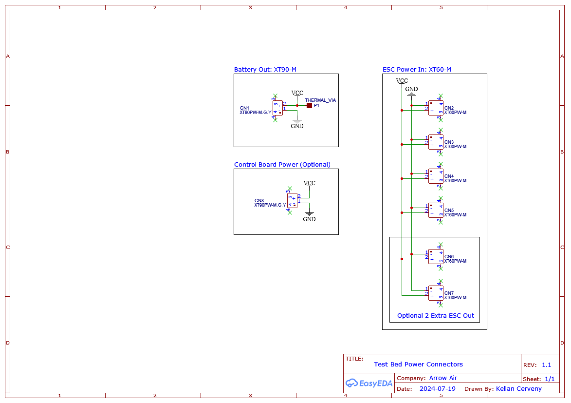
The World’s Easiest Schematic?
This board is going to solve an admittedly simple problem. We wanted to remove the extra cables and harnessing from the test bed drone and replace it with a single PCB. If done properly, this should reduce the weight of the payload and simplify troubleshooting in the future. If possible, I should also allow for this PDB to used on future designs even if the drone’s design changes.
The power input comes directly from the drone’s battery through an XT-90 connector. This power is then routed to four motor electronic speed controllers (ESCs), with the possibility of introducing two more in the future. I also recommended that we offer a power output to the drone’s control board, which we could choose to use in the future.

The World’s Hardest PCB?
In my experience, most of the challenge in designing a PCB comes at the beginning. Solving circuits, choosing components, and understanding the system’s tolerances take a lot of the mental load. Once I get to the PCB, its mostly a game of finding a nice layout and playing connect the dots.
I think this project is notable because it was the exact opposite. I went in already knowing that this board was going to use XT-90 and XT-60 connectors, and its intention was to only connect all of the power and ground lines together. That is what made the schematic so simple.
Now, I had to solve a a much harder question. How do I connect this much DC power without it going up in flames?
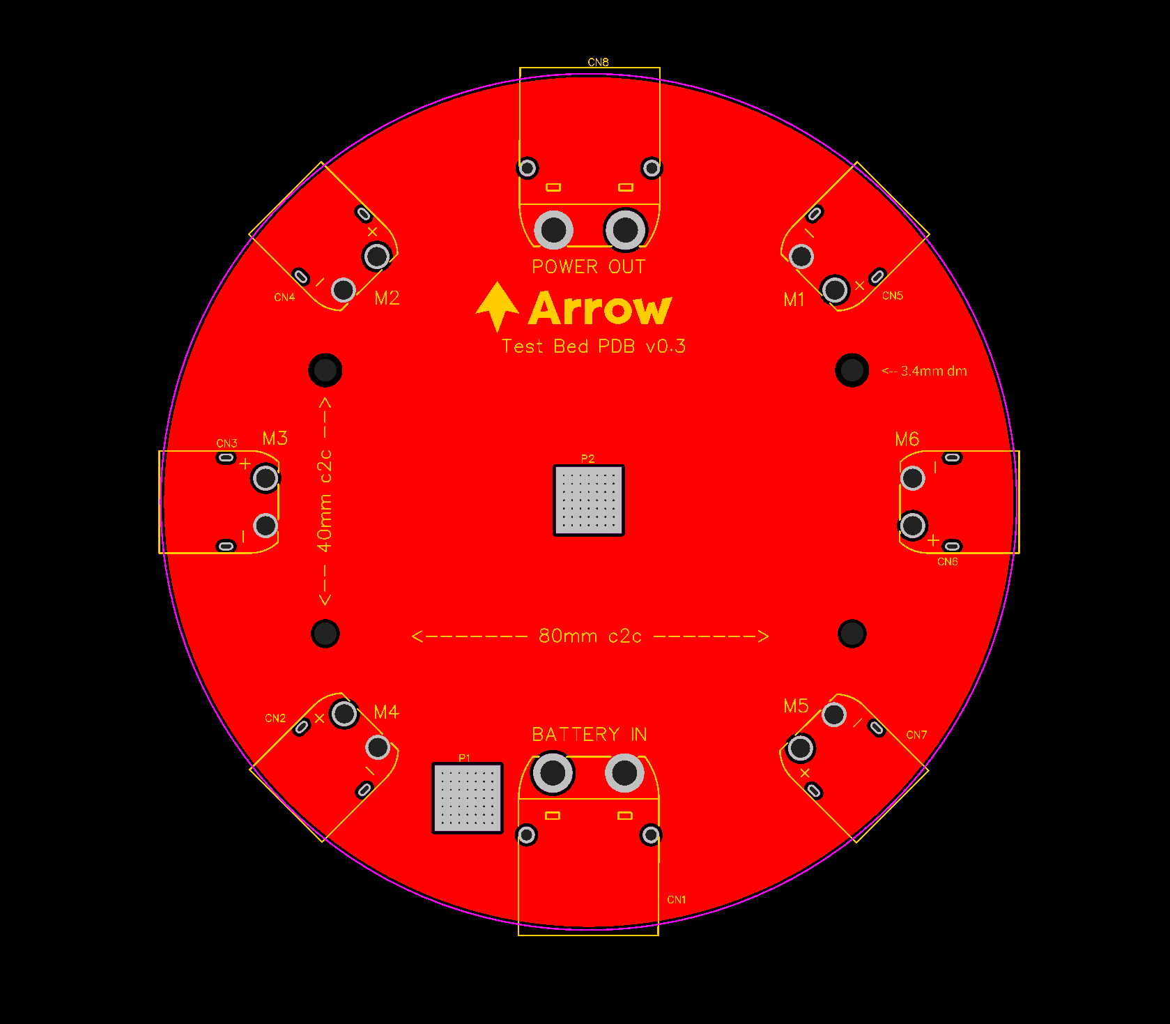
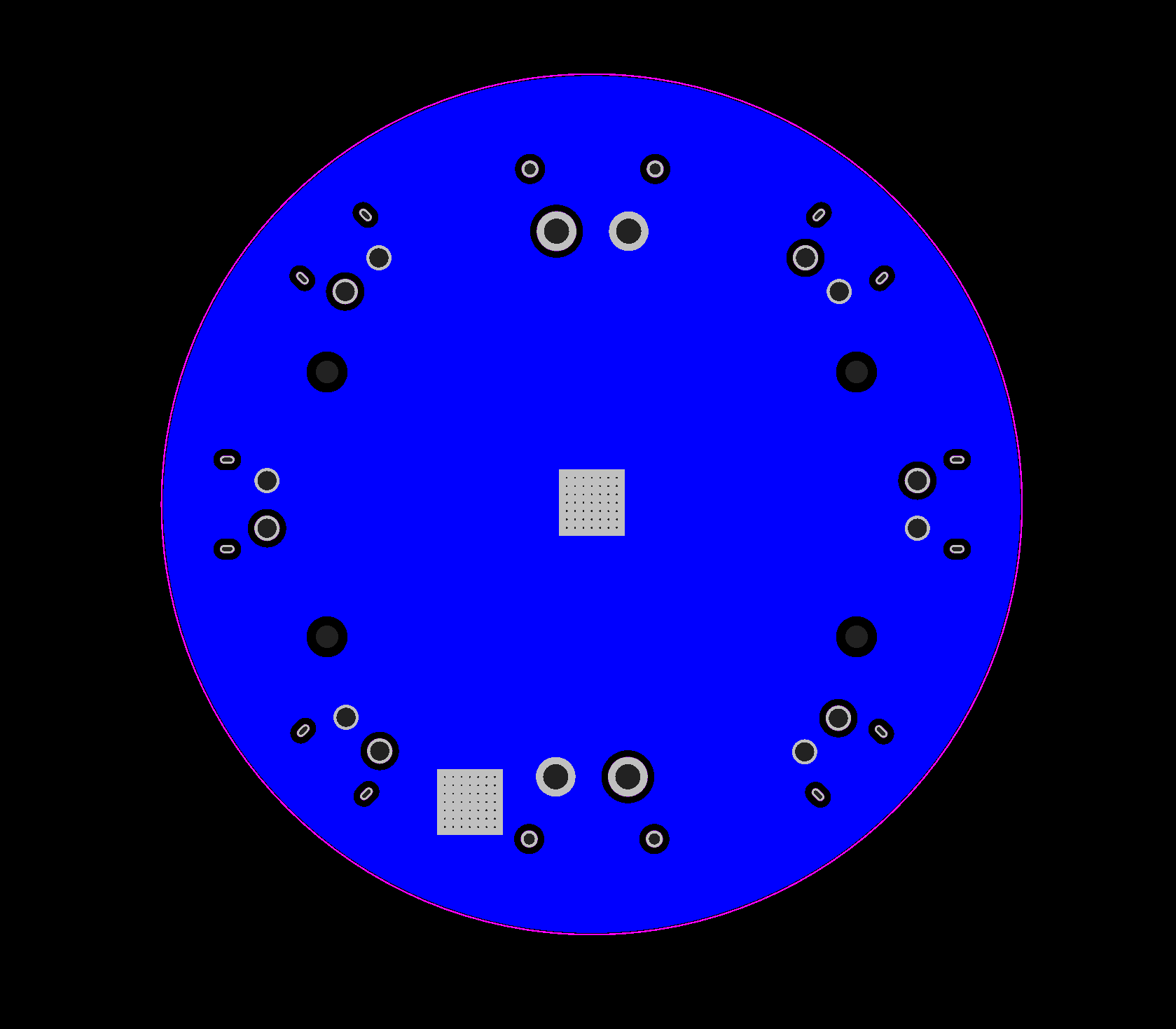
Because there were only two nets on this board (Power In and Ground), I decided to make this a two-sided PCB in which all of the top layer was a ground power plane and the opposite was power. Doing so simplified the connections considerably, and expanded the amount of copper that each net could access.
But this did not solve all of my concerns.
- Can this board sustain a maximum of 150 Amps DC?
- Will this board heat evenly as power flows?
- Will the produced heat affect the internal substrate?
- Should I include copper bus bars to mitigate the reliance on the PCB?


As an aside, I find documentation on group projects to be really important. When I design my PCBs I always make an effort to include information that might be important for other engineers. Here I included silkscreen labels for the center-to-center distance between the mounting holes, and those holes’ diameters. They may go unused, but the information needed is always packaged with the board.